IPC-7525 Rev L General Guideline and Formulas. This includes differences for tin lead and lead-free solder paste overprint two-print and step stencil designs.
2
The IPC stencil guidelines are the most commonly used and are a good starting point however they do not take into account outside variables that regularly come up in all manufacturing lines such as environmental conditions oven profile printing variables squeegee pressure under-board support squeegee speed etc.
. TERMS AND DEFINITIONS FOR INTERCONNECTING AND PACKAGING ELECTRONIC CIRCUITS. Available Formats Availability Priced From in USD Secure PDF ℹ Immediate download 8900 Add to Cart Printed Edition. Historical IPC 7525A-2007 Stencil Design Guidelines This document provides guidelines for the design and fabrication of stencils for solder paste and surface-mount adhesive.
Stencil design for various surface-mount technology as well as mixed technology with through-hole or flip chip components is discussed. These guidelines detail the differences for tin-lead and lead-free solder paste overprint two-print and step stencil designs. 12 foil_thickness 2.
Stencil Design Guidelines This standard establishes the guidelines for the design and fabrication of stencils for solder paste and surface mount adhesive with discussion on through-hole mixed technology and includes the differences for tin lead and lead-free solder paste overprint two-print and step stencil designs. STENCIL AND MISPRINTED BOARD CLEANING HANDBOOK. Fine and ultra-fine pitch lands together with other advanced packages place new demands on stencil cleaning.
November 2021 IPC-7525C 1 Stencil Design Guidelines 10 SCOPE 11 Purpose This document provides guidance for the design and fabrication of stencils for solder paste and surface-mount adhesive. Much of the content is based on the experience of stencil designers fabricators and users. Contribution is from screen-printing process where stencil design plays major role if considered other screen-printing parameters are optimized on which this paper is focused on.
During the initial Stage of Stencil design it is imperative to arrest these problems. According to IPC design guidelines 7525B there should be 89mm 035 keep-out between the step down and the aperture in the step down area for every 025mm 001 of step height. An example would be a ceramic BGA where it is necessary t.
IPC-7525 Revision C November 2021 - Stencil Design Guidelines. ASSOCIATION CONNECTING ELECTRONICS INDUSTRIES Stencil Design Guidelines IPC-7525A Stencil Design Guidelines Developed by the Stencil Design Task Group 5-21e of the Assembly and Joining Processes Committee 5-20 of IPC Users of this publication are encouraged to participate in the development of future revisions. GENERIC STANDARD ON PRINTED BOARD DESIGN.
View all product details Historical Track It Language. Much of the content is based on the experience of stencil designers fabricators and users. This document provides guidance for the design and fabrication of stencils for solder paste and surface-mount adhesive.
DESIGN AND ASSEMBLY PROCESS IMPLEMENTATION FOR BOTTOM TERMINATION COMPONENTS. Institute of Printed Circuits Table of Contents Abstract General Product Information Standards Referenced By This Book Standards Referencing This Book Cross Sell Categories associated with this Standard. IPC T 50.
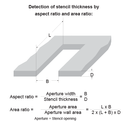
According to this IPC-7525L standard two factors that help a designer to calculate and estimate the quality of his stencil design are. Download IPC 7525A pdf. Applicable for Leaded SMD PiINTRODUCTION.
The handbook serves as a guide to users or prospec-tive users of stencilmisprint cleaning technology. IPC 7525B-2011 Stencil Design Guidelines Provides guidelines for the design and fabrication of stencils for solder paste and surface mount adhesive with discussion on through-hole and mixed technology. IPC-7525A - Stencil Design Guidelines 352 Step-Up Stencil This type stencil is useful when it is desirable to print thicker solder paste in a small portion of the stencil.
It is intended as a guideline only. 5700 price reduced by 56 Quantity. Stencil Design Guidelines 1 PURPOSE This document provides guides for the design and fabrica-tion of stencils for solder paste and surface-mount adhe-.
Normally there is not sufficient spacing on many SMT assemblies having very small components and normal SMT components to allow this much keep-out. Design of Stencil should comply with IPC-7525A. Stencil Design Guidelines Developed by the Stencil Design Task Group 5-21e of the Assembly and Joining Processes Committee 5-20 of IPC Users of this publication are encouraged to participate in the development of future revisions.
Width of bridge between apertures. 13 Overview Cleaning of stencils and misprinted PCBs has taken an increasingly important role in surface mount technology. Stencil manufacturing and design PBGA package - Square aperture with side length equal to the diameter of pads - Foil thickness considerations as below - CSP take care of particle diameter in paste CBGA package - overprinting - Min.
IPC 3000 Lakeside Drive Suite 309S Bannockburn Illinois 60015-1249 Tel 847 6157100 Fax 847 6157105. IPC-7525 Stencil Design Guidelines ASSOCIATION CONNECTING ELECTRONICS INDUSTRIES 2215 Sanders Road Northbrook IL 60062-6135 Tel. More info This document provides guidelines for the design and fabrication of stencils for solder paste and surface mount adhesive with discussion on through-hole and mixed technology.
It is intended as a guideline only. B Current Add to Watchlist STENCIL DESIGN GUIDELINES Available format s. STENCIL DESIGN FOR BGA PACKAGES O.
The step-upstep-down stencil is a special development for the adjustment of solder paste quantity fulfilling the needs of placement and soldering. However we also introduce another factor that not directly mention in IPC document is solder paste volume estimation. IPC 7525A Stencil Design Guidelines standard by Association Connecting Electronics Industries 02012007 This document has been replaced.
View the most recent version. This paper is set on guidelines to minimize the process complexities and issues in production using above standard. Aspect Ratio and Area Ratio.

Ipc 7525 A Stencil Design Guidelines Pdf Docer Com Ar

Ipc 7525 A Stencil Design Guidelines Pdf Docer Com Ar

Ipc 7525a 2007 Stencil Design Guidelines
Smd Stencils Design Aid Multi Circuit Boards

Ipc 7525 A Stencil Design Guidelines Pdf Docer Com Ar

Ipc 7528b Table Of Contents Ipc 7528b Table Of Contents Pdf Pdf4pro
Ipc 7525c Stencil Design Guidelines

Ipc 7525 A Stencil Design Guidelines Pdf Docer Com Ar
0 comments
Post a Comment